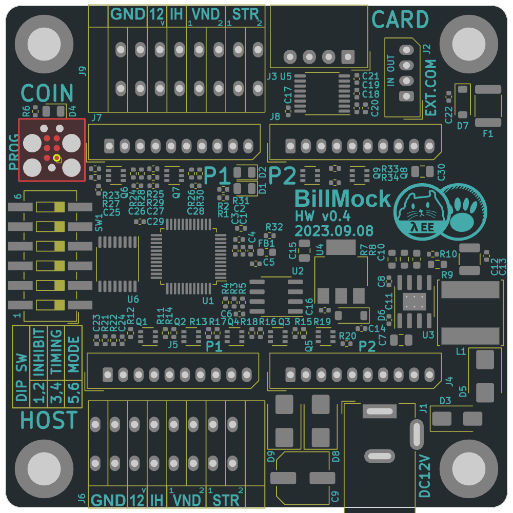
Overview
"Billmock" is a system designed to manipulate the currency payment I/O signals that arcade machines receive based on specific conditions. It is primarily used in South Korean arcade machines for tasks such as installing credit card reader or enabling programmable operations for sequential tasks based on various conditions.
To configure it for desired settings on-site, "Billmock" allows preconfigured I/O remapping adjustments through DIP switches. In terms of wiring, it is installed between the HOST GAME PCB and the bill acceptor device.
Hardware
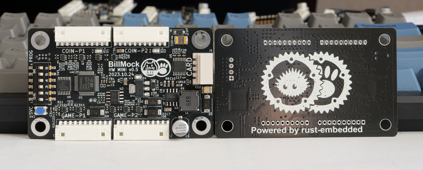 The hardware revision currently adopted for final mass production is 0.5-MINI, and the software development is also progressing according to this version.
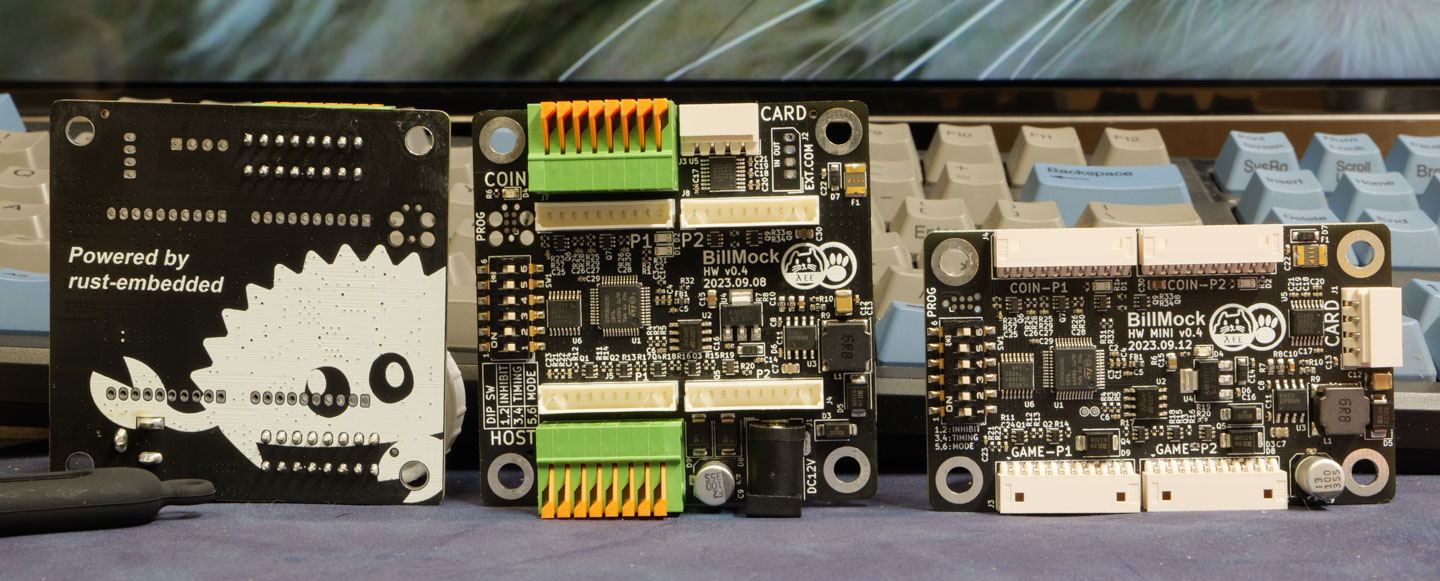 There are three previous hardware revisions available: 0.2, 0.3, and 0.4. The development is focused on compatibility with versions 0.3 and 0.4, which are the ones actively in use. Detailed hardware schematics are here
BillMock-HW-RELEASE
Application
The firmware software has been developed in Rust, as opposed to the de facto C language. While the choice to use Rust is partly based on trust in its reliability, it also serves the purpose of validating its suitability for embedded systems intended for mass production. Therefore, hope to maintain the firmware source code as a precedent, akin to an example code.
License
This program and the accompanying materials are made available under the terms of the Apache Software License 2.0 which is available at Apache Software License 2.0, or the MIT license which is available at MIT License
Also all of codes are based one MIT or Apache Software License 2.0. But some common *.toml files are based on CC0-1.0 license. (Example Cargo.toml)
DIP Switch

Overview
| SW # | SW Name | Anotation |
|---|---|---|
1 | INHIBIT0 | Inhibit Override - Player 1 |
2 | INHIBIT1 | Inhibit Override - Player 2 |
3 | TIMING0 | Timing Override (50 ms Std) |
4 | TIMING1 | Timing Override (100 ms Std) |
5 | MODE0 | Application mode |
6 | MODE1 | Application mode |
Inhibit override dip switch configuration
Inhibit0 (1) | Inhibit1P (2) | Configuration |
|---|---|---|
0 | 0 | Normal (No force overriding) |
1 | 0 | Override inhibit on 1P as force |
0 | 1 | Override inhibit on 2P as force |
1 | 1 | Override inhibit globally |
- By override for each player by dip switch setting, regardless of game I/O signal, it is forcibly set to inhibit state.
- Even if there is no override in the dip switch settings, if inhibit is enabled on the host game I/O side, inhibit for each player is activated.
- This Inhibit DIP Switch setting can be used to prohibit currency acquisition of a device that has under the maintenance in the field engineer.
Timing configuration
TIMING0 (3) | TIMING1 (4) | Configuration |
|---|---|---|
0 | 0 | Auto |
1 | 0 | Force 50mS active low |
0 | 1 | Force 100mS active low |
1 | 1 | Force 200mS active low |
-
Timing SW
00(Auto), for the active-low output signal, the pulse duration provided by serial communication or the pulse duration measurement value of parallel communication (legacy coin & bill acceptor) is set separately according to the signal source. If both are unavailable, the default value (100 mS) will be used. -
Timing SW
01,10,11ignores the pulse duration of all signal sources and fixes it to one of 50 mS, 100 mS, and 200 mS and outputs it.
Application mode dip switch configuration
MODE0 (5) | MODE1 (6) | Swap status | Special Feature |
|---|---|---|---|
0 | 0 | Start Signal | No, Start signal bypass to host(game pcb) side output |
1 | 0 | Start Signal | Yes, Start signal decide vend output direction for payment income from serial communication |
0 | 1 | Jam Signal | No, Jam signal bypass to jam(game pcb) side output |
1 | 1 | Invalid | DisplayRom, disallow any other action |
-
MODE0 (5) : Special feature disable or enable
-
MODE1 (6) : Swap
startandjaminput signal on vend side, default definition is start. -
00: BypassStartNormal mode with bypass start (default value). Start signal bypass to host(game pcb) side output.
-
01: StartButtonDecideSerialToVendSpecial mode with start button mocked. Start signal decide vend output direction for payment income from serial communication.
-
10: BypassJamNormal mode with bypass JAM (swapped logically). JAM signal bypass to host(game pcb) side output.
-
11: DisplayRom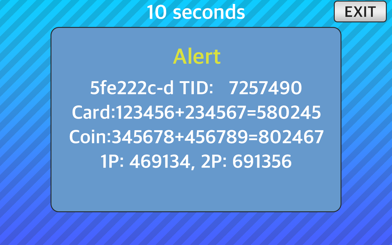
- It displays information about BillMock's firmware, the card terminal's TID, and accumulated card and bill (coin) counts. It can be used as an alternative to a magnetic coin meter.
- Upon exiting this mode, DisplayHwInfo will display hardware information.
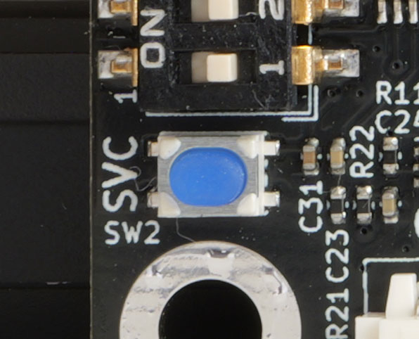
- When the SVC button is held for more than 10 seconds, the counts are reset to 0 through the Counter Reset feature.
- If the connected card terminal's TID changes, the accumulated card count will be reset to 0. For detailed information, please refer to DisplayRom Detailed Information.
Application Logic
The simplified program and signal input-output flow are as follows:
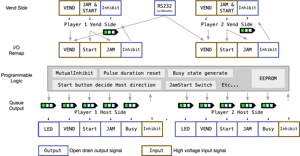
Overview of Operation
This device is designed to enhance payment systems by storing, manipulating, and delaying input/output signals from currency payment devices (such as credit card readers, coin acceptors, bill validators) before connecting them to the GAME I/O PCB.
By configuring DIP switch settings and making appropriate wiring changes, you can guide the setup between the desired currency payment device and the GAME I/O PCB. This device enables the following configurations:
- Installing a credit card reader on an existing game machine.
- Using both a credit card reader and a bill validator (or coin acceptor) on 1P (Player 1) in an existing game machine.
- Managing 1P/2P (Player 1/Player 2) when using one card reader and one bill validator (or coin acceptor) on an existing game machine upon pressing the start button.
- Managing 1P/2P (Player 1/Player 2) when using one bill validator (or coin acceptor) on an existing game machine upon pressing the start button.
- Override output pulse duration based DIP switch configuration and input signal.
- Display accumulated card / paper(or coin) count instead of magnetic coin meter.
- Allowing users to make more complex modifications to input/output signals through code customization.
DisplayRom

-
To view such information during normal operation, please check and configure the DIP SWITCH execution mode.
-
The information will appear for 10 seconds, divided into four lines, displaying details about ROM and the program:
-
Line 1:
{Git Hash} {TID}- Git Hash: The shortened git commit hash of the BillMock firmware program billmock-app-rs.
- TID: The unique Terminal ID of the card terminal. It is a value set in the card terminal when connecting it to the payment gateway (PG). It is also a unique identifier in the PG's system.
-
Line 2:
Cards: {1P Count} + {2P Count} = {Credit Sum}- 1P Count: Accumulated clock counts for Player 1 based on pre-configured clock settings and consumer payments on the card terminal.
- 2P Count: Accumulated clock counts for Player 2 based on pre-configured clock settings and consumer payments on the card terminal.
- Credit Sum: The sum of 1P Count and 2P Count, representing credits processed by the card terminal.
-
Line 3:
Bills: {1P Count} + {2P Count} = {Coin Sum}- 1P Count: Accumulated clock counts for Player 1 based on bill acceptor or coin acceptor clock settings and consumer payments.
- 2P Count: Accumulated clock counts for Player 2 based on bill acceptor or coin acceptor clock settings and consumer payments.
- Coin Sum: The sum of 1P Count and 2P Count, representing currency processed by the bill acceptor or coin acceptor.
-
Line 4:
1P: {1P Sum Count}, {2P Sum Count}- 1P Sum Count: The total clock counts accumulated for Player 1 by the card terminal and bill acceptor (or coin acceptor).It's the sum of 1P Count from the second and third lines.
- 2P Sum Count: The total clock counts accumulated for Player 2 by the card terminal and bill acceptor (or coin acceptor).It's the sum of 2P Count from the second and third lines.
-
-
All count numbers are displayed in 6 digits (0 ~ 999,999). If the count exceeds 1,000,000, it will be displayed as 000,000, and the next count after that will increment normally, such as 000,001.
-
This feature is available starting from firmware version
0.2.0and hardware0.4orMini 0.4and later. It is not available for previous hardware versions. -
From hardware version 0.5 or Mini 0.5 onwards, you can use the SVC button by pressing it briefly.
DisplayRom
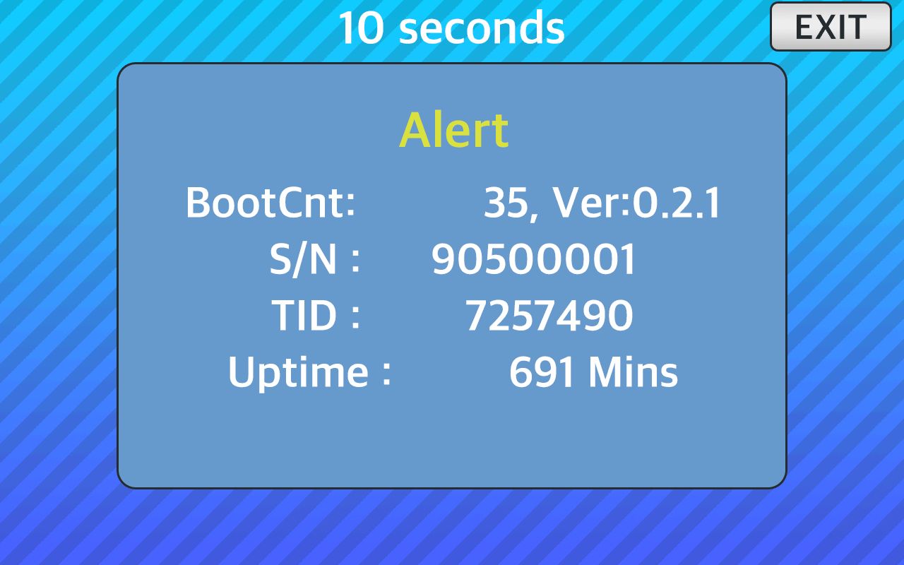
-
To view such information during normal operation, please check and configure the DIP SWITCH execution mode.
-
The information will appear for 10 seconds, divided into four lines, displaying details about ROM and the program:
-
Line 1 :
{Boot Cnt} Ver:{x.y.z}- Boot Cnt: Number of boots for the BillMock hardware. It increments by 1 each time the device is powered off and on.
- x.y.z: Firmware version of the BillMock program billmock-app-rs.
-
Line 2 :
S/N : {Serial Number}- Serial Number: Unique serial number assigned to the BillMock hardware during mass production.
-
Line 3 :
TID : {TID}- TID: The unique Terminal ID of the card terminal. It is a value set in the card terminal when connecting it to the payment gateway (PG). It is also a unique identifier in the PG's system.
-
Line 4 :
Uptime : {Uptime} Mins- Uptime: Represents the duration the BillMock hardware has been powered on, measured in minutes.
-
-
This feature is available from firmware version
0.2.1and hardware version0.4orMini 0.4onwards. It is not supported on earlier hardware versions. -
From hardware version 0.5 or Mini 0.5 onwards, you can use the SVC button by pressing 2 seconds.

-
This feature is available starting from firmware version
0.2.0and hardware0.4orMini 0.4and later. It is not available for previous hardware versions. -
When exiting DispRom through the DIP switch on hardware version
0.4orMini 0.4and above, the display is also shown.
Counter Reset
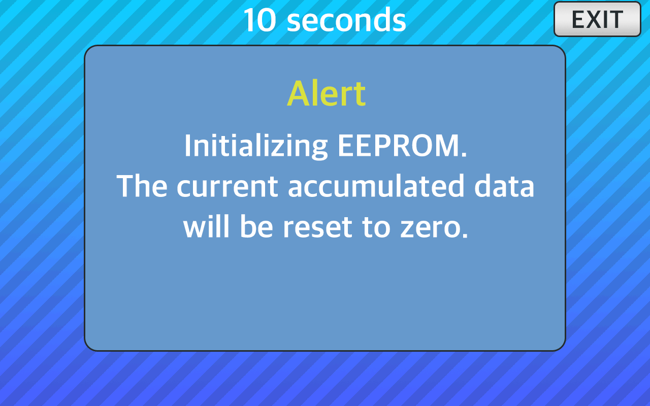
-
The warning message appears for 10 seconds, and the ROM contents are already initialized when the warning message is displayed.
-
The counts displayed in DispRom for
P1 Card,P2 Card,P1 Coin,P2 Coinare reset to 0, but information such as boot count and uptime remains unaffected. -
This feature is available starting from firmware version
0.3.1and hardware version0.5orMini 0.5. The SVC button on hardware version0.5orMini 0.5must be held for more than 10 seconds to activate this feature.
Machine installation
When connecting to actual arcade machines, there are two installation options available, each with its own advantages and disadvantages. It is recommended to test both methods and select the one that best suits your needs.
MOLEX Harness
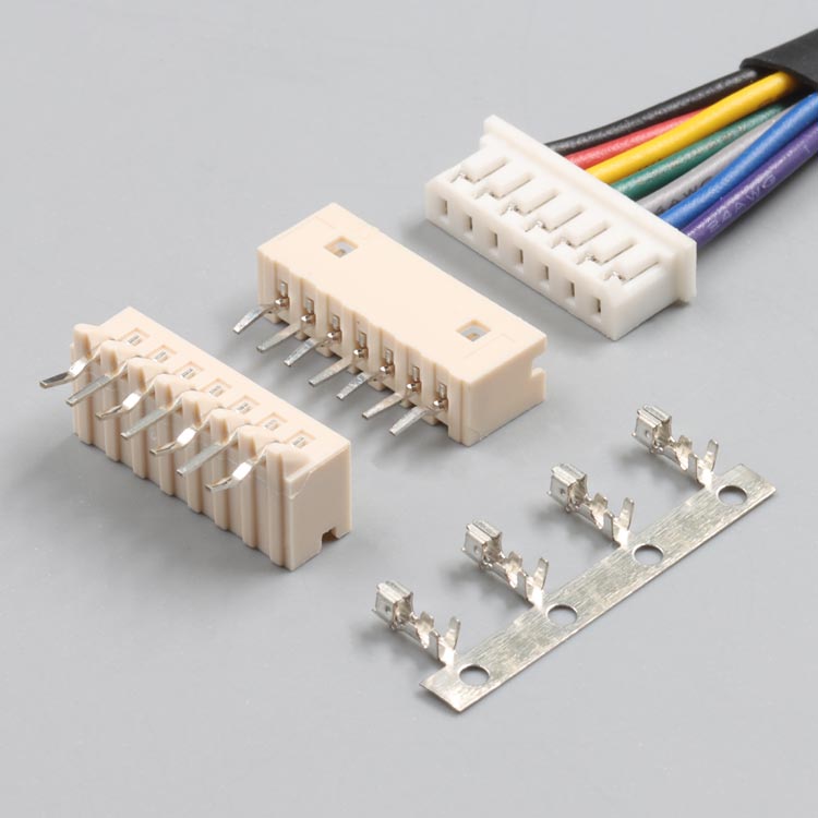
- Prepare the Harness Based on the Pinout Chart
- Connect
Cut previous harness and connect to terminal
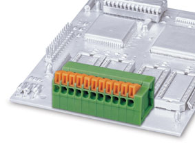
- Assuming there is some flexibility in the cable length, cut the cable at the installation point.
- Strip the insulation from both ends of the cut cable, leaving approximately 1cm (10mm) of exposed wire.
- While pressing the orange latch on the top/bottom terminal, securely insert the stripped wire into the hole.
- Note: Typically, the top side should be connected to the actual currency payment device, while the bottom side should be connected to the GAME I/O PCB.
- Note: Ensure there is some length flexibility in the existing cables.
- Note: Only cables conforming to UL/CUL standards with AWG20 or higher and AWG26 or lower can be used with these terminals.
Difference between two hardware types
| Mini types | regular version |
|---|---|
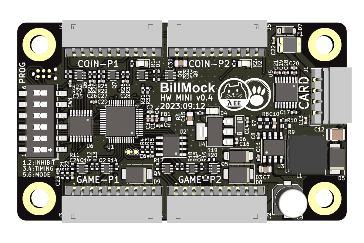 | 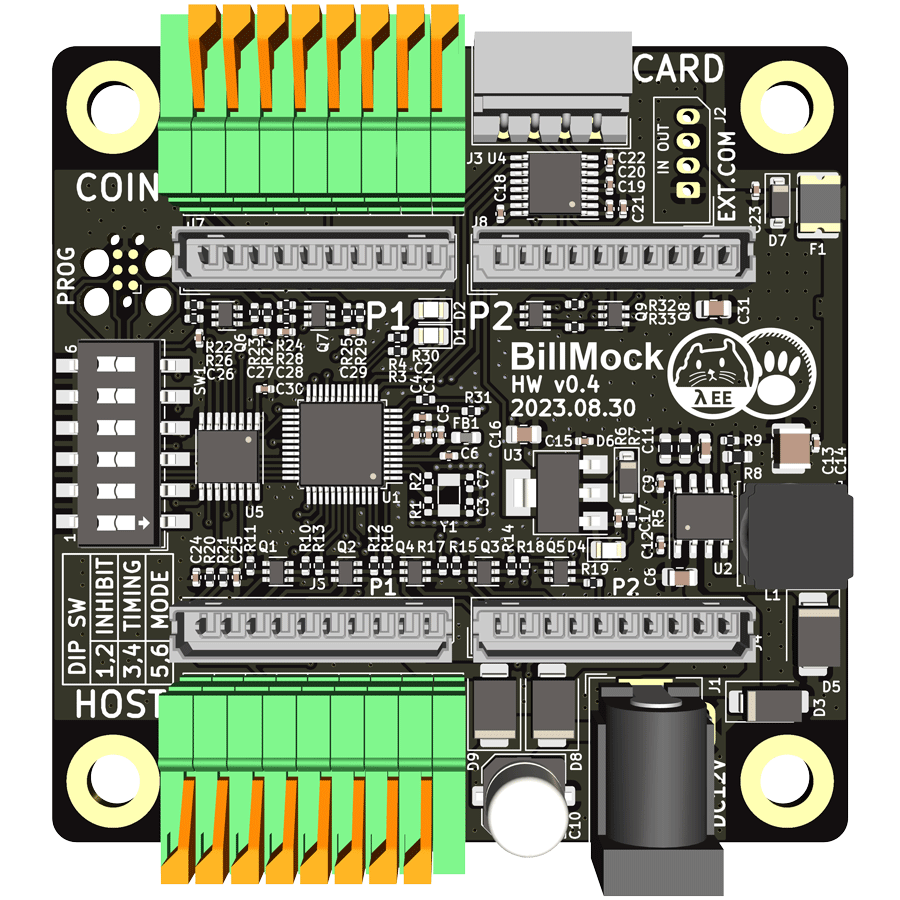 |
BillMock hardware comes in two different variants. There is the smaller rectangular-shaped BillMock Mini (Rectangular) and the square-shaped BillMock (Square) with terminals and a DC jack on the top and bottom.
The Mini version removes the terminals, DC jack, and additional RS232 port compared to the standard version. It comes at a lower price point and is easier to install if you already have the harness prepared. In situations where harness configuration is complex and it's more convenient to connect directly to the terminals on-site, the standard version may be suitable.
However, for most on-site installations, we recommend the Mini version as it offers greater efficiency, especially when using pre-configured harnesses, making the installation process smoother.
Table of Contents
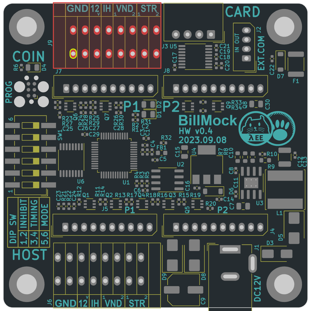
At the top, there are connectors for the Vend Side, which includes bill paper acceptors, coin acceptors, credit card reader, and similar currency validators.
At the bottom, connectors are placed for the Host Side, which interfaces with the mainboard of the actual arcade machine, such as the GAME I/O PCB.
On the left and right sides, you'll find identical connectors arranged in a decalcomania pattern. The connectors on the left are designated for Player 1, while those on the right are for Player 2.
With this pattern of connectors, it's easy to connect wires to the connectors during actual installation and operation by referring to the layout.
BillMock Mini
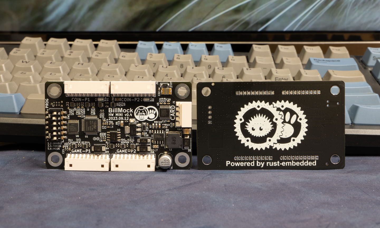
| Front side | Back side |
|---|---|
 | 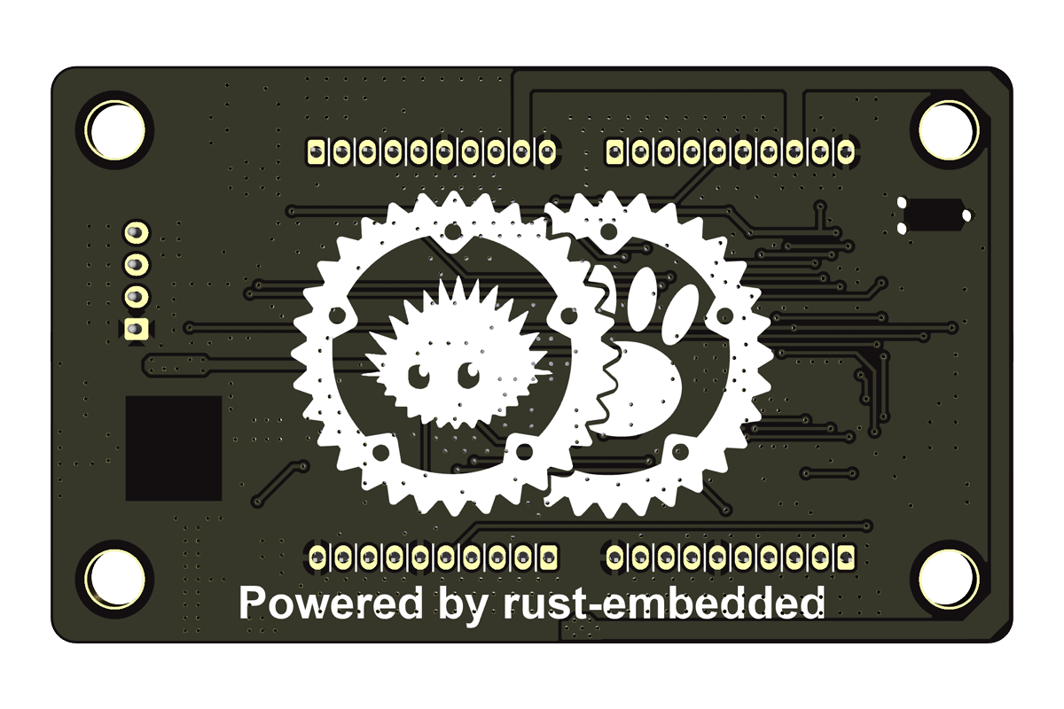 |
Pin map overview
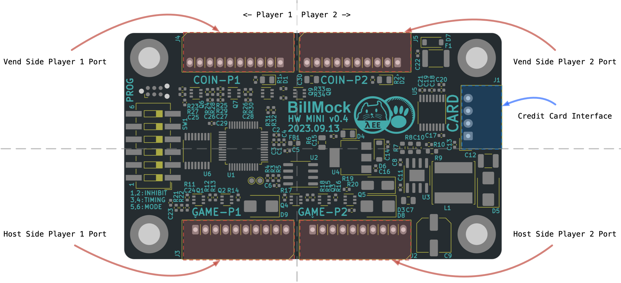
At the top, there are connectors for the Vend Side, which includes bill paper acceptors, coin acceptors, credit card reader, and similar currency validators.
At the bottom, connectors are placed for the Host Side, which interfaces with the mainboard of the actual arcade machine, such as the GAME I/O PCB.
On the left and right sides, you'll find identical connectors arranged in a decalcomania pattern. The connectors on the left are designated for Player 1, while those on the right are for Player 2.
With this pattern of connectors, it's easy to connect wires to the connectors during actual installation and operation by referring to the layout.
From a conceptual perspective, in the existing wiring, the connectors that were originally connected from top to bottom are each separated and connected to the upper and lower connectors. The hardware and software manage the communication between these upper and lower connectors. This design was intentional during the connection setup.
Simplified Connection of BillMock Mini
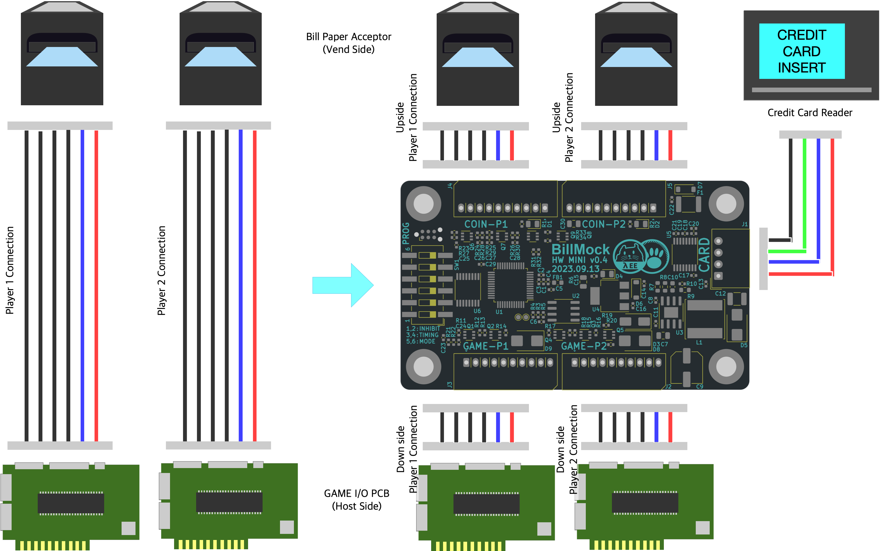
- WARN : The wire shapes are symbolic representations and do not indicate the actual wire colors used in the image. Please refer to detailed pinouts in the respective pages.
This configuration involves installing this PCB (BillMock) between the existing bill acceptor (or coin acceptor) on the top and the GAME I/O PCB on the bottom, with a harness connection.
In some cases, additional wiring work may be required, but considering the widely used bill acceptor wiring in South Korea, you can prepare the harness and connect it accordingly.
Specifications
| Product name | BillMock |
| Manufacturer | GPARK Co., Ltd. |
| Country | South Korea |
| Dimension | 75.0 mm * 45.0 mm |
| MCU | STM32G030C8 |
| MCU Spec | ARM Cortex-M0+ 64Mhz CPU, 8KiB SRAM, 64KiB Flash |
| Software | Embassy-rs written in rust |
| Power Input | 12V 2A |
| Pouwer Output | 5V (Peak 2.2A 300mS trip, 1.1A nominal MAX) - Credit card reader power |
- WARN : The input power allows up to 16V, but please be cautious as it is directly passed through to the bill handling device.
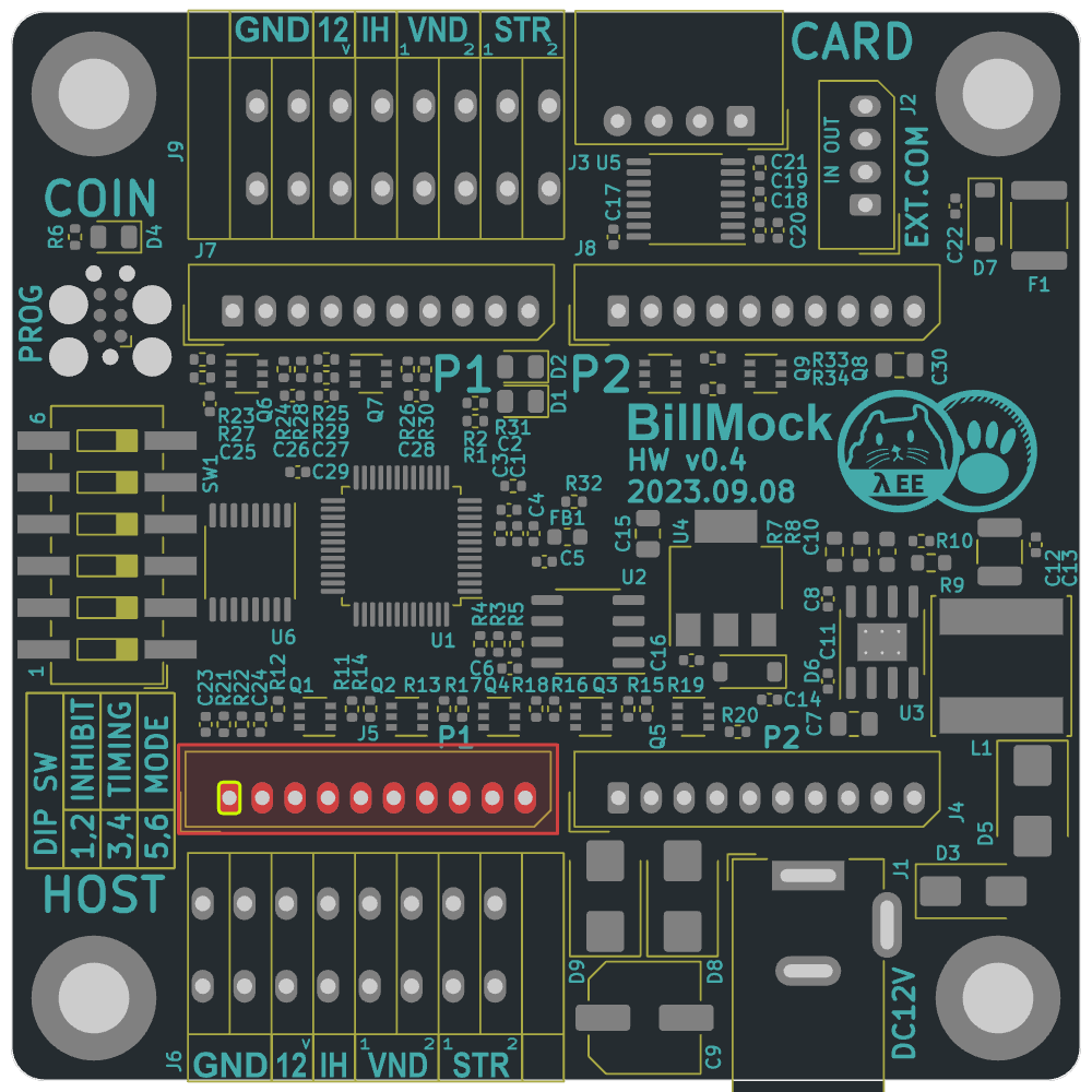
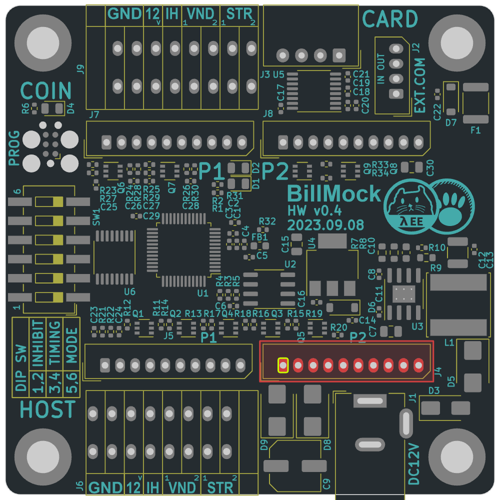
Vend side port map
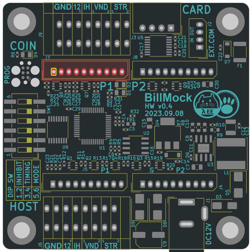
Vend Side Player 1 Port (left)
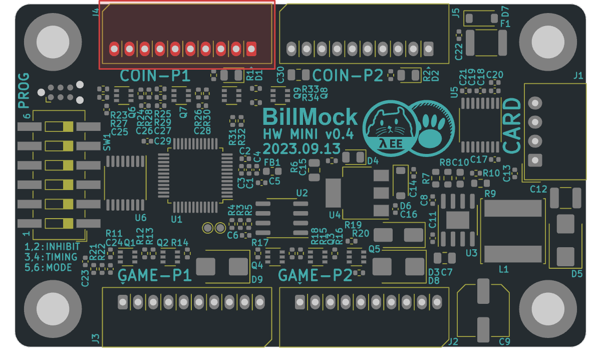
| Designator | J4 |
| Player 1 side existing coin and bill acceptor port | |
| Connector | Molex 53014-10xx |
| Housing | Molex 51004-10xx |
| Crimp | Molex 50011 |
| Pin # | Pin Name | Annotation |
|---|---|---|
1 | N/C | Not Connected |
2 | VEND | Bill acceptor Coin Insertion Signal |
3 | N/C | Not Connected |
4 | START | Start Button Input Signal |
5 | INHIBIT | Bill acceptor Inhibit (Deactivate) Output Signal |
6 | GND | Bill acceptor - Pole Power (Input/Output) |
7 | N/C | Not Connected |
8 | 12V | Bill acceptor + Pole Power (Input/Output) |
9 | 12V | Bill acceptor + Pole Power (Input/Output) |
10 | GND | Bill acceptor - Pole Power (Input/Output) |
- Pins are counted from the left.
- START can be changed to JAM based on DIP switch settings
Vend Side Player 2 Port (right)
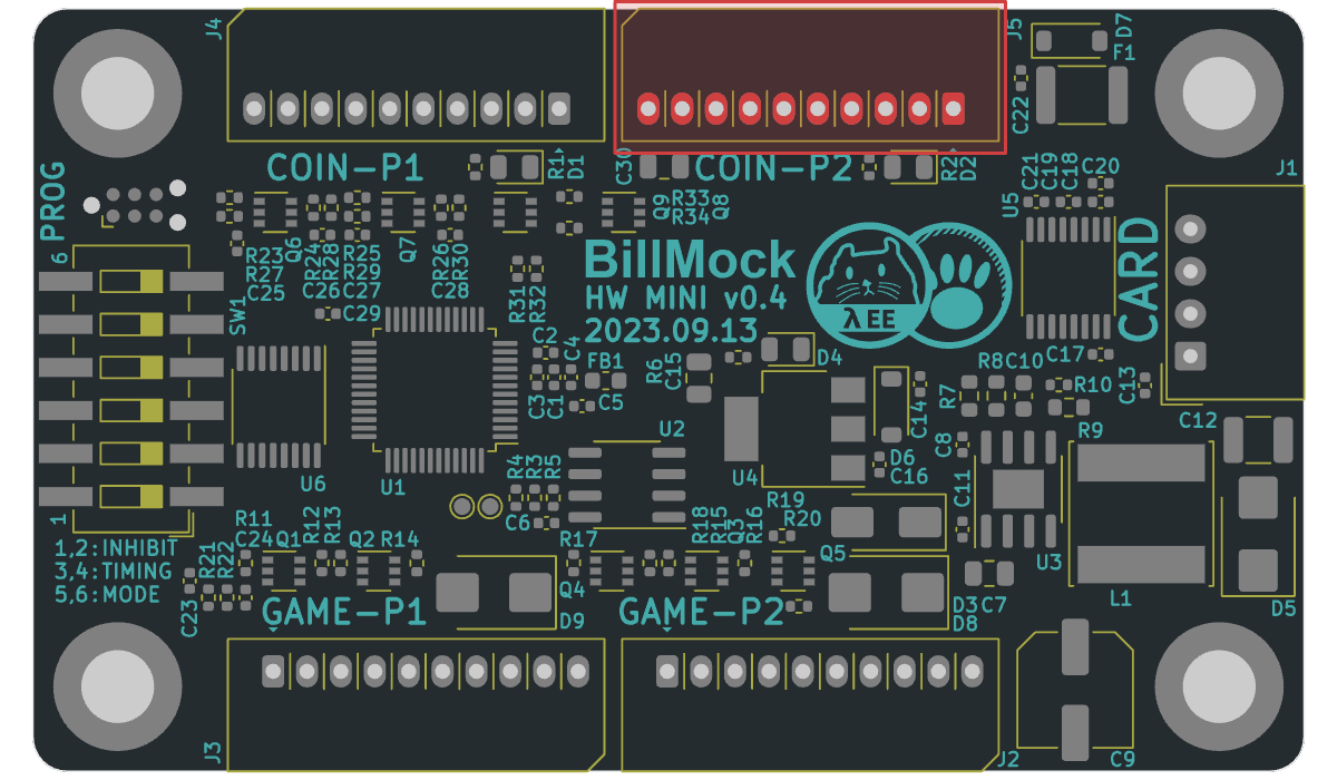
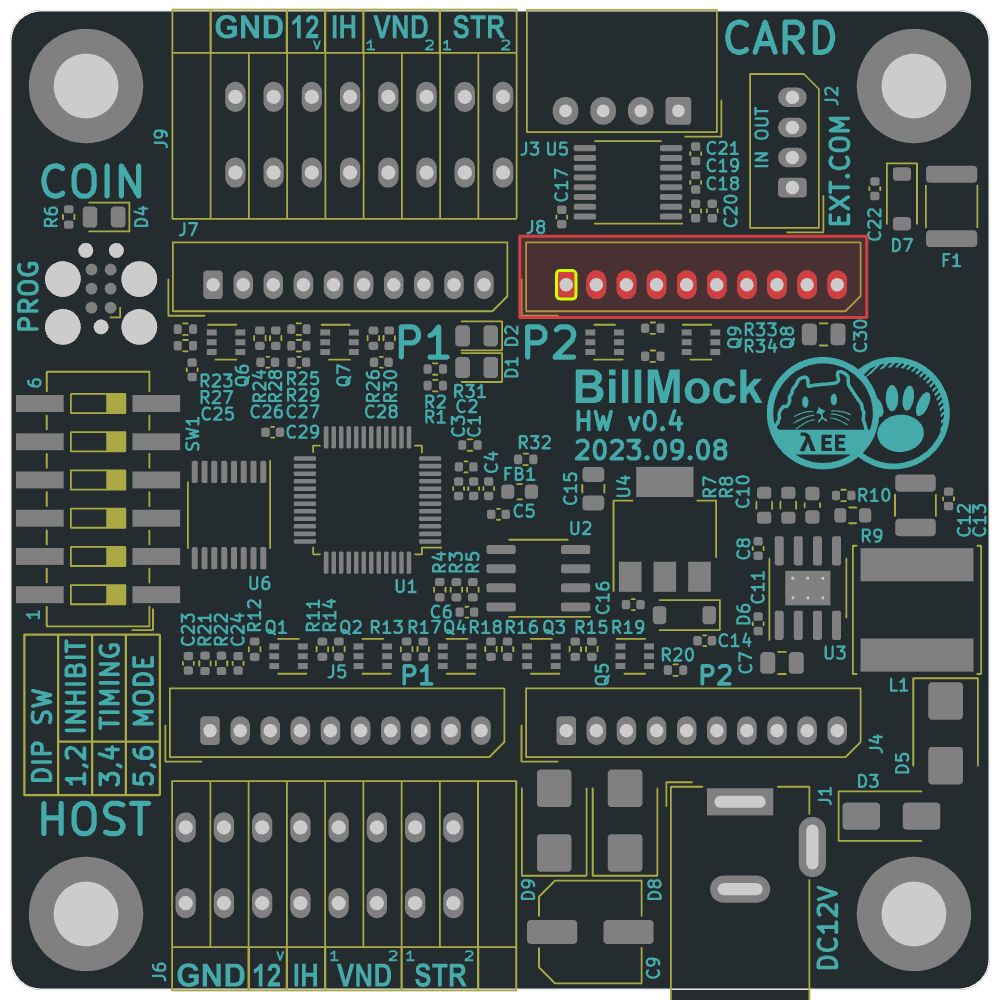
| Designator | J5 |
| Player 2 side existing coin and bill acceptor port | |
| Connector | Molex 53014-10xx |
| Housing | Molex 51004-10xx |
| Crimp | Molex 50011 |
| Pin # | Pin Name | Annotation |
|---|---|---|
1 | N/C | Not Connected |
2 | VEND | Bill acceptor Coin Insertion Signal |
3 | N/C | Not Connected |
4 | START | Start Button Input Signal |
5 | INHIBIT | Bill acceptor Inhibit (Deactivate) Output Signal |
6 | GND | Bill acceptor - Pole Power (Input/Output) |
7 | N/C | Not Connected |
8 | 12V | Bill acceptor + Pole Power (Input/Output) |
9 | 12V | Bill acceptor + Pole Power (Input/Output) |
10 | GND | Bill acceptor - Pole Power (Input/Output) |
- Pins are counted from the left.
- START can be changed to JAM based on DIP switch settings
Host side 핀 아웃
Host Side Player 1 Port (left)
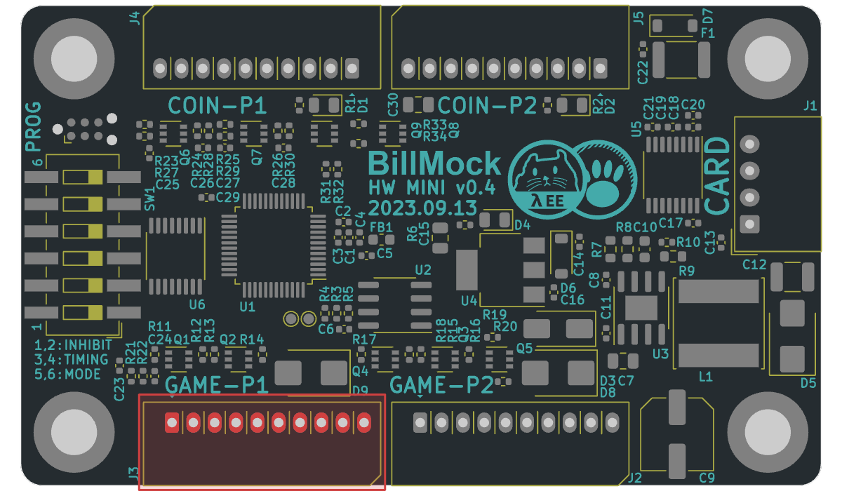
| Designator | J3 |
| Emulated Player 1 side connector towards the GAME IO side | |
| Connector | 141R-2.54-8P |
| Pin # | Pin Name | Annotation |
|---|---|---|
1 | V1-BUSY | Emulated Busy state Output Signal |
2 | V1-VEND | Emulated Bill acceptor 1P Coin Insertion Output Signal |
3 | V1-JAM | Emulated JAM Output Signal |
4 | V1-START | Emulated 1P Start Button Output Signal |
5 | V1-INHIBIT | Inhibit Input Signal from 1P GAME I/O |
6 | N/C | Not Connected |
7 | N/C | Not Connected |
8 | 12V | Product + Pole Power Input |
9 | 12V | Product + Pole Power Input |
10 | GND | Product - Pole Power Input |
- Pins are counted from the right.
- You can also input power directly into BillMock-HW through
12VandGNDpins. - The power pins from this port cannot be used for power output. When power input to this port is blocked, reverse voltage does not flow.
- The "Busy" output signal remains active low from the moment a payment signal is received from the credit card or when the VEND input signal goes active low until the VEND output signal toggles and completes.
Host Side Player 2 Port (right)
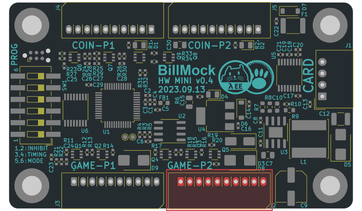
| Designator | J2 |
| Emulated Player 2 side connector towards the GAME IO side | |
| Connector | 141R-2.54-8P |
| Pin # | Pin Name | Annotation |
|---|---|---|
1 | V1-BUSY | Emulated Busy state Output Signal |
2 | V1-VEND | Emulated Bill acceptor 2P Coin Insertion Output Signal |
3 | V1-JAM | Emulated JAM Output Signal |
4 | V1-START | Emulated 2P Start Button Output Signal |
5 | V1-INHIBIT | Inhibit Input Signal from 2P GAME I/O |
6 | N/C | Not Connected |
7 | N/C | Not Connected |
8 | 12V | Product + Pole Power Input |
9 | 12V | Product + Pole Power Input |
10 | GND | Product - Pole Power Input |
- Pins are counted from the right.
- You can also input power directly into BillMock-HW through
12VandGNDpins. - The power pins from this port cannot be used for power output. When power input to this port is blocked, reverse voltage does not flow.
- The "Busy" output signal remains active low from the moment a payment signal is received from the credit card or when the VEND input signal goes active low until the VEND output signal toggles and completes.
Port - Miscellaneous
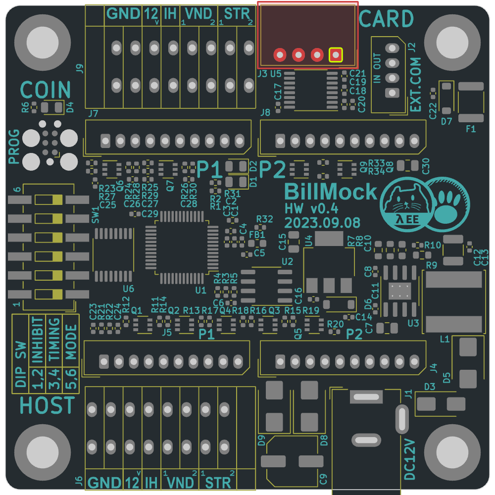
Credit Card Reader Port
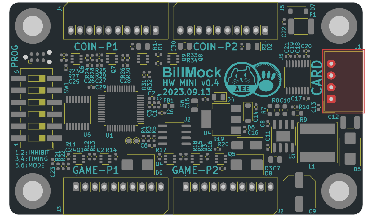
|
|
- 5V Power output maximum rating is Peak 2.2A 300mS trip, 1.1A nominal MAX.
Program debugging (SWD/JTAG)
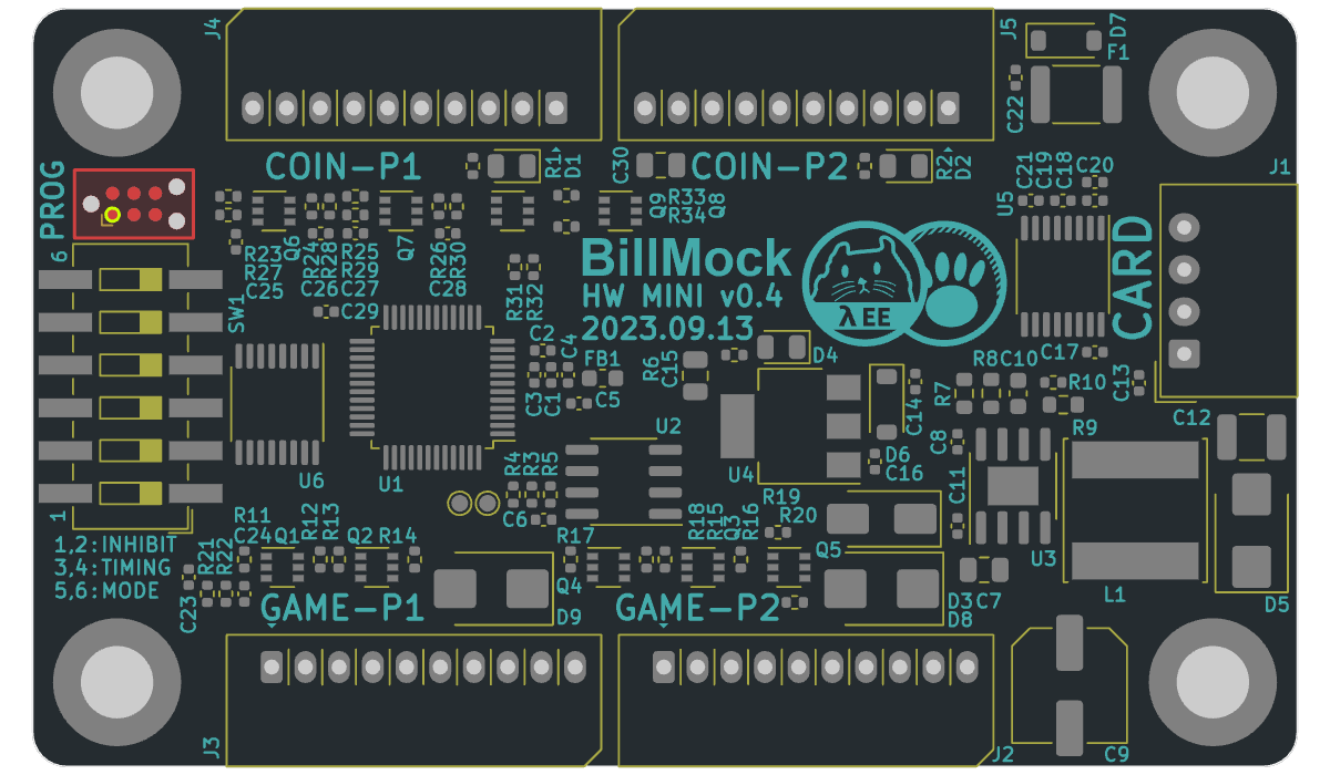
| Role | STM32 SWD |
| Connector | TC2030 |
- Detail information is in BillMock-HW-RELEASE
BillMock
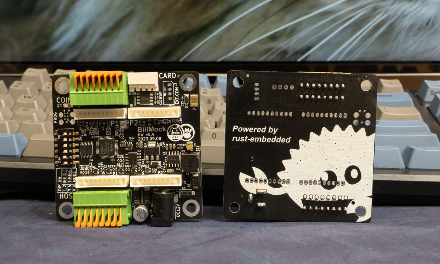
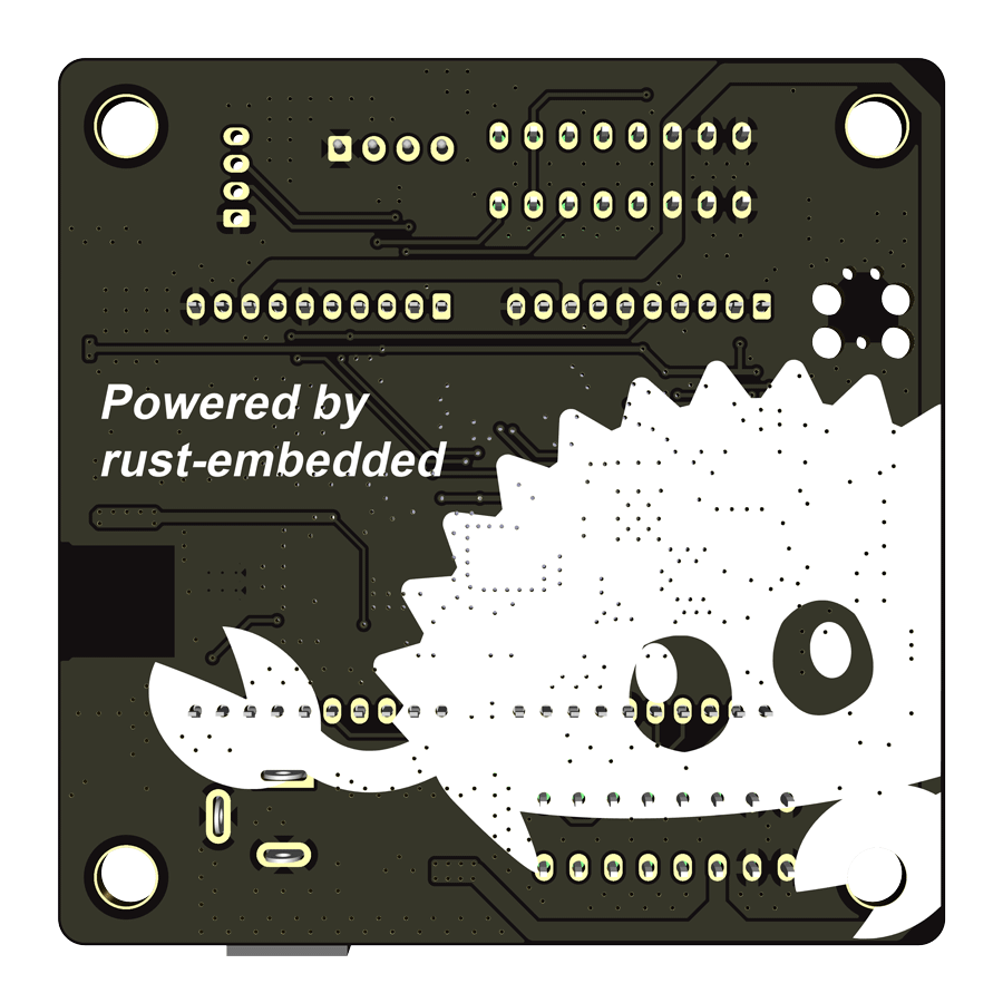
| Front side | Back side |
|---|---|
 |  |
Pin map overview
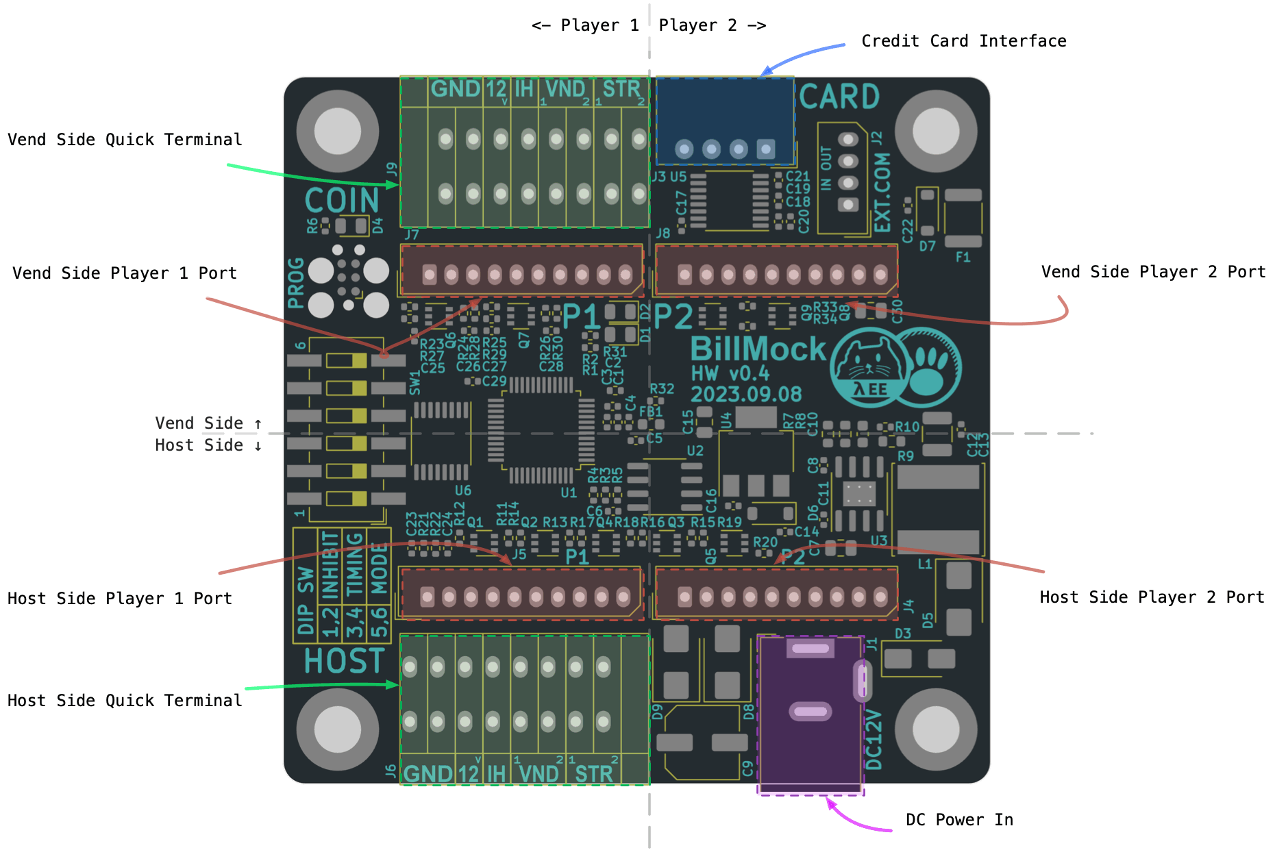
At the top, there are connectors for the Vend Side, which includes bill paper acceptors, coin acceptors, credit card reader, and similar currency validators.
At the bottom, connectors are placed for the Host Side, which interfaces with the mainboard of the actual arcade machine, such as the GAME I/O PCB.
On the left and right sides, you'll find identical connectors arranged in a decalcomania pattern. The connectors on the left are designated for Player 1, while those on the right are for Player 2.
With this pattern of connectors, it's easy to connect wires to the connectors during actual installation and operation by referring to the layout.
From a conceptual perspective, in the existing wiring, the connectors that were originally connected from top to bottom are each separated and connected to the upper and lower connectors. The hardware and software manage the communication between these upper and lower connectors. This design was intentional during the connection setup.
In addition to these connectors, there are connectors for power supply, an additional RS232 connector for debugging, and an SWD (JTAG) connector for program debugging.
Simplified Connection of BillMock
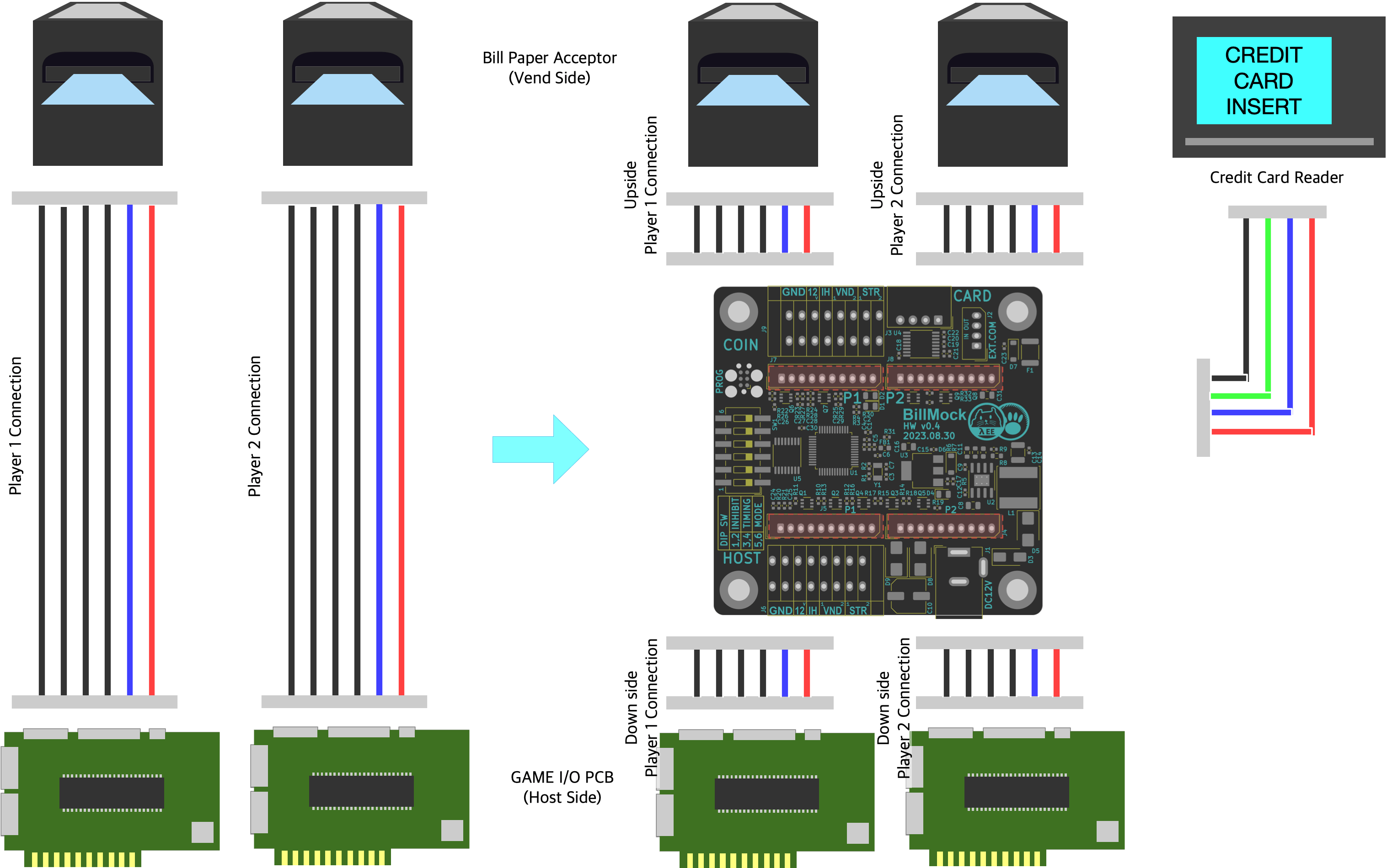
- WARN : The wire shapes are symbolic representations and do not indicate the actual wire colors used in the image. Please refer to detailed pinouts in the respective pages.
This configuration involves installing this PCB (BillMock) between the existing bill acceptor (or coin acceptor) on the top and the GAME I/O PCB on the bottom, with a harness connection.
In some cases, additional wiring work may be required, but considering the widely used bill acceptor wiring in South Korea, you can prepare the harness and connect it accordingly.
Unlike the BillMock Mini version, you can also perform wiring work through terminals. For more details, please refer to the Machine Installation document.
Additionally, the terminal pinouts are slightly different from standard Molex connectors, so please review this document for details on the top and bottom terminals:
Specifications
| Product name | BillMock |
| Manufacturer | GPARK Co., Ltd. |
| Country | South Korea |
| Dimension | 65.0 mm * 65.0 mm |
| MCU | STM32G030C8 |
| MCU Spec | ARM Cortex-M0+ 64Mhz CPU, 8KiB SRAM, 64KiB Flash |
| Software | Embassy-rs written in rust |
| Power Input | 12V 2A |
| Pouwer Output | 5V (Peak 2.2A 300mS trip, 1.1A nominal MAX) - Credit card reader power |
- WARN : The input power allows up to 16V, but please be cautious as it is directly passed through to the bill handling device.
Vend side port map
Vend Side Quick Terminal
|
|
|
- Pins are counted from the left.
- You can also input power directly into BillMock-HW through
12VandGNDpins. - While it's more convenient to strip tde insulation from tde cable in tde middle and tden connect it to tde terminal,
- It's recommended, whenever possible, to use a cable type that comes pre-equipped for the connection.
- START1/2 can be changed to JAM based on DIP switch settings
Vend Side Player 1 Port (left)
|
|
|
- Pins are counted from the left.
- START can be changed to JAM based on DIP switch settings
Vend Side Player 2 Port (right)
|
|
|
- Pins are counted from the left.
- START can be changed to JAM based on DIP switch settings
Host side port map
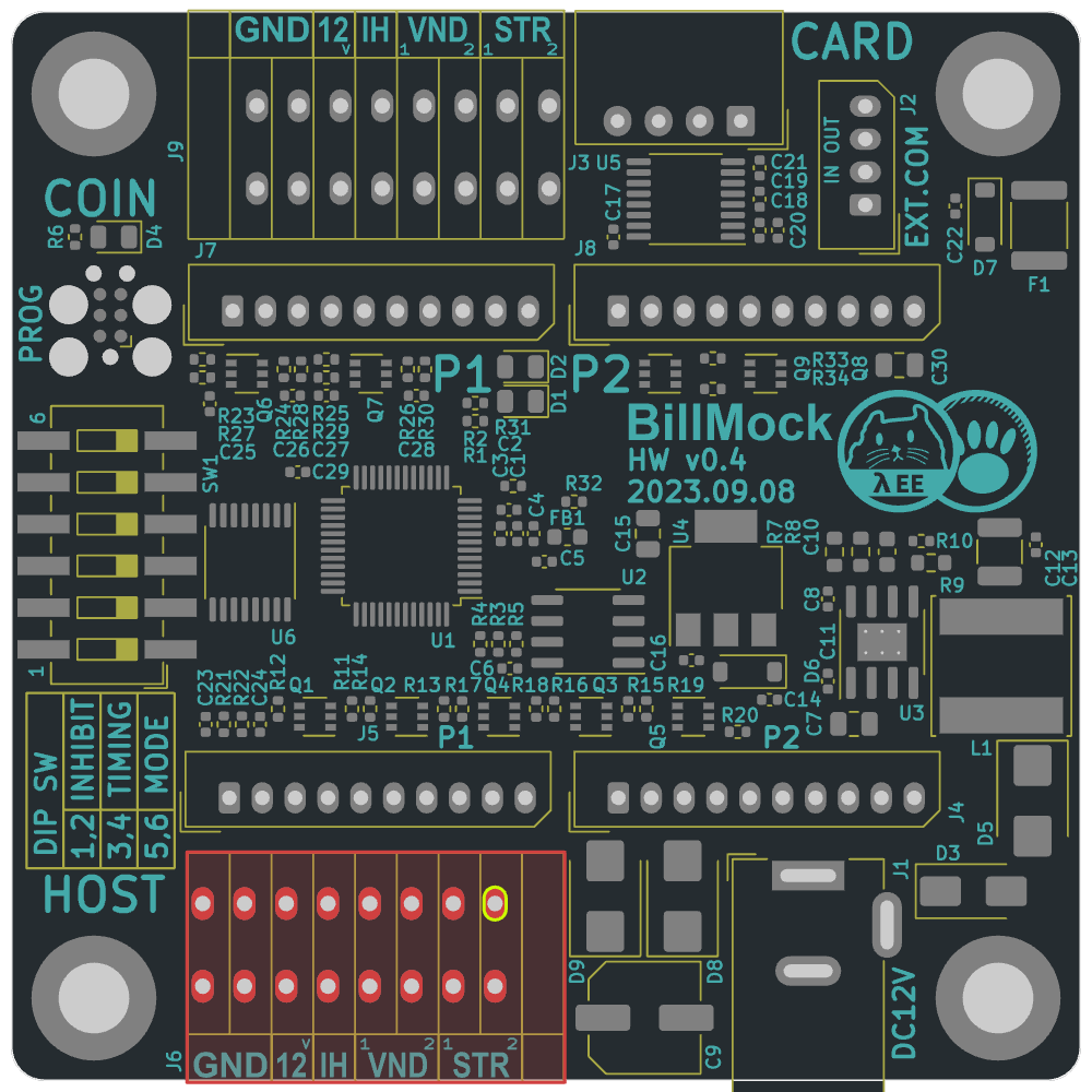
Host Side Quick Terminal
|
|
|
- Pins are counted from the left.
- You can also input power directly into BillMock-HW through
12VandGNDpins. - While it's more convenient to strip tde insulation from tde cable in tde middle and tden connect it to tde terminal,
- It's recommended, whenever possible, to use a cable type that comes pre-equipped for the connection.
Host Side Player 1 Port (left)
|
|
|
- Pins are counted from the left.
- You can also input power directly into BillMock-HW through
12VandGNDpins. - The power pins from this port cannot be used for power output. When power input to this port is blocked, reverse voltage does not flow.
- The "Busy" output signal remains active low from the moment a payment signal is received from the credit card or when the VEND input signal goes active low until the VEND output signal toggles and completes.
Host Side Player 2 Port (right)
|
|
|
- Pins are counted from the left.
- You can also input power directly into BillMock-HW through
12VandGNDpins. - The power pins from this port cannot be used for power output. When power input to this port is blocked, reverse voltage does not flow.
- The "Busy" output signal remains active low from the moment a payment signal is received from the credit card or when the VEND input signal goes active low until the VEND output signal toggles and completes.
Port - Miscellaneous
Credit Card Reader Port
|
|
|
- 5V Power output maximum rating is Peak 2.2A 300mS trip, 1.1A nominal MAX.
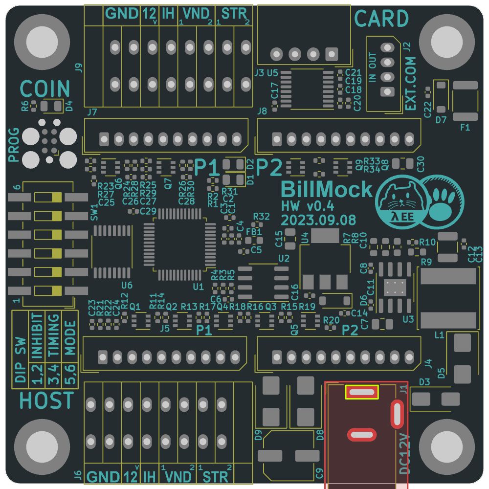
DC Power Jack
|
|
|
- 12V input is recommended (maximum 16V).
- In addition to the bottom DC jack, it is also recommended to receive power through the 10-pin Molex ports on the bottom left (J5) and bottom right (J4).
- Using the top terminal (J9) or the top 10-pin Molex (J7/J8) for power input is not recommended.
Program debugging (SWD/JTAG)
|
|
|
- Detail information is in BillMock-HW-RELEASE
Developer Manual
Write In Rust
Used rust experimentally.
This repository is aiming three goal. One for development of production firmware and second is making a proof of concept that rust embedded is usable for actual embedded production. And last goal is setting some example about production-rust-embedded-code.
The software code is in billmock-app-rs , except NDA related code.
Software
Card Terminal Connectivity in actual environment
The firmware being developed is based on KICC's ED-785 terminal for mass production. However, in accordance with the NDA agreement, the code related to this is not present in the public codebase. Instead, it is managed separately through dependency injection. Therefore, the publicly available source code contains only example protocol code that does not actually perform any real operations.
Develop Environment
※ It might available with Windows, but in this document only consider Debian-Linux.
apply USB (stlink-v2/3) permission rule to ignore root access
# refer https://calinradoni.github.io/pages/200616-non-root-access-usb.html
sudo tee /etc/udev/rules.d/70-st-link.rules > /dev/null <<'EOF'
# ST-LINK V2
SUBSYSTEMS=="usb", ATTRS{idVendor}=="0483", ATTRS{idProduct}=="3748", GROUP="plugdev", MODE="660", TAG+="uaccess", SYMLINK+="stlinkv2_%n"

# ST-LINK V2.1
SUBSYSTEMS=="usb", ATTRS{idVendor}=="0483", ATTRS{idProduct}=="374b", GROUP="plugdev", MODE="660", TAG+="uaccess", SYMLINK+="stlinkv2-1_%n"
SUBSYSTEMS=="usb", ATTRS{idVendor}=="0483", ATTRS{idProduct}=="3752", GROUP="plugdev", MODE="660", TAG+="uaccess", SYMLINK+="stlinkv2-1_%n"

# ST-LINK V3
SUBSYSTEMS=="usb", ATTRS{idVendor}=="0483", ATTRS{idProduct}=="374d", GROUP="plugdev", MODE="660", TAG+="uaccess", SYMLINK+="stlinkv3loader_%n"
SUBSYSTEMS=="usb", ATTRS{idVendor}=="0483", ATTRS{idProduct}=="374e", GROUP="plugdev", MODE="660", TAG+="uaccess", SYMLINK+="stlinkv3_%n"
SUBSYSTEMS=="usb", ATTRS{idVendor}=="0483", ATTRS{idProduct}=="374f", GROUP="plugdev", MODE="660", TAG+="uaccess", SYMLINK+="stlinkv3_%n"
SUBSYSTEMS=="usb", ATTRS{idVendor}=="0483", ATTRS{idProduct}=="3753", GROUP="plugdev", MODE="660", TAG+="uaccess", SYMLINK+="stlinkv3_%n"
EOF
apply rules and reboot linux
sudo usermod -a -G plugdev $USER
sudo udevadm control --reload-rules
sudo udevadm trigger
sudo reboot
Necessary apt package for rust embedded
# necessary for basic software development environment
sudo apt install curl git build-essential -y
# build.rs uses libgit2-sys to get commit hash
sudo apt install pkg-config libssl-dev -y
# for knurling-rs/probe-run
sudo apt install libusb-1.0-0-dev libudev-dev -y

# Install rustc/rustup/cargo for rust development environment
curl --proto '=https' --tlsv1.2 -sSf https://sh.rustup.rs | sh

# Install probe-run for debug/flash firmware binary on target board.
cargo install probe-run

# Install cargo-binutils for analyze mem/flash usage.
cargo install cargo-binutils
rustup component add llvm-tools-preview
Build
cargo build
pmnxis@lmabdaDeb ~/Develop/billmock-app-rs master cargo build
info: syncing channel updates for 'nightly-2023-08-24-x86_64-unknown-linux-gnu'
info: latest update on 2023-08-24, rust version 1.74.0-nightly (249595b75 2023-08-23)
info: downloading component 'cargo'
info: downloading component 'clippy'
info: downloading component 'llvm-tools'
info: downloading component 'rust-docs'
info: downloading component 'rust-src'
info: downloading component 'rust-std' for 'thumbv6m-none-eabi'
info: downloading component 'rust-std'
info: downloading component 'rustc'
info: downloading component 'rustfmt'
info: installing component 'cargo'
info: installing component 'clippy'
info: installing component 'llvm-tools'
info: installing component 'rust-docs'
info: installing component 'rust-src'
info: installing component 'rust-std' for 'thumbv6m-none-eabi'
info: installing component 'rust-std'
info: installing component 'rustc'
info: installing component 'rustfmt'
Updating crates.io index
Updating git repository `https://github.com/embassy-rs/embassy.git`
Cargo Run
pmnxis@lmabdaDeb ~/Develop/billmock-app-rs master cargo run
Finished dev [optimized + debuginfo] target(s) in 0.06s
Running `probe-run --chip STM32G030C8Tx --log-format '{t} [{L}][ {f}:{l} ] {s}' target/thumbv6m-none-eabi/debug/billmock-app-rs`
(HOST) INFO flashing program (45 pages / 45.00 KiB)
(HOST) INFO success!
────────────────────────────────────────────────────────────────────────────────
0.000000 [DEBUG][ fmt.rs:130 ] rcc: Clocks { sys: Hertz(16000000), apb1: Hertz(16000000), apb1_tim: Hertz(16000000), ahb1: Hertz(16000000) }
+-----------------------------------------------------------+
Firmware Ver : billmock-app-rs 0.1.2
Git Hash : bf976acd38633f7204e9423def8b5b062e0a0ad3
Git Datetime : 2023-09-17 20:55:10 +0900 | bf976ac
+-----------------------------------------------------------+
0.004272 [TRACE][ fmt.rs:117 ] USART: presc=1, div=0x0000008b (mantissa = 8, fraction = 11)
0.004638 [TRACE][ fmt.rs:117 ] Using 16 bit oversampling, desired baudrate: 115200, actual baudrate: 115107
1.006286 [WARN ][ serial_device.rs:156 ] The module use a example library. It may not work in real fields.
OUT[ LED2-Indicator] : Low
OUT[ LED1-Indicator] : Low
Dependency Injection for card reader
To build with NDA features (GPARK Limited or own secret dependency), need adding following command on each cargo command.
build, run or any other cargo command.
# dependency injection from git repository
# CAUTION , this should be work but not working
--config "patch.'https://github.com/pmnxis/billmock-app-rs.git'.billmock-plug-card.git = \"https://github.com/user_name/repo_name.git\""

# dependency injection from local repository
# this works
--config "patch.'https://github.com/pmnxis/billmock-app-rs.git'.billmock-plug-card.path = \"../repo_name\""
In this repository, experimentally utilize dependency injection that the 'patch' function of 'cargo' to coexist both NDA code and open source example code.
Hardware

There are currently four hardware revisions available: 0.2, 0.3, 0.4, and 0.4 Mini. Development is being carried out specifically for the 0.4 and 0.4 Mini revisions, which are the ones that are actually usable.
To check pin mappings or installation details, please refer to the desired section in the table of contents on the left.
For detailed hardware schematics, you can refer to BillMock-HW-RELEASE.
Hardware design
BillMock hardware schematic repository (only pdf) : BillMock Hardware PDF Release
The schematic printed in PDF is distributed under CC BY-SA 3.0, but the actual Gerber files and project files are private.
v 0.4 Mini (2023-09-12 or 2023-09-13)
v 0.4 (2023-09-08)
v 0.3 (2023-08-11) - DEPRECATED
v 0.2 (2023-06-13) - DEPRECATED
Hardware License Information
The original data for the circuit diagram is under a private license, but the PDF schematic is distributed under the CC-BY-SA 3.0 license. Therefore, data such as gerbers and the Bill of Materials (BOM) used in production will not be disclosed at all. Additionally, circuits created based on this schematic (PDF) must adhere to the following conditions:
Please provide proper attribution when using it for commercial purposes.
-
Attribution: You must give appropriate credit, provide a link to the license, and indicate if changes were made. You may do so in any reasonable manner, but not in any way that suggests the licensor endorses you or your use.
-
ShareAlike: If you remix, transform, or build upon the material, you must distribute your contributions under the same license as the original.
Translation Note: This text appears to describe the licensing terms and conditions related to the hardware, particularly regarding the use of schematic data.
